|
|
|
|
Global SMT & Packaging March 2006 Fact and Fiction in lead-Free soldering - Part IThe electronics industry’s transition to lead-free soldering has been characterised by misapprehensions about the properties that are important in a lead-free solder and about the consequences for soldering processes and solder joint reliability. In this article the realities that have emerged from the practical implementation of lead-free soldering are reviewed and their implications for alloy selection considered. Particular attention is given to the benefits of replacing tin-lead, which behaves as near perfect eutectic, with lead-free solders that also behave as a eutectic. Keith Sweatman, Nihon Superior, Osaka, Japan - ksweatman@aol.com Misapprehensions and misinformation
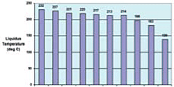
The trauma is perhaps understandable given that the industry has been asked to give up the material that has been the basis for the assembly of electronic circuitry since there was such a thing as electronic circuitry. Though far from a perfect material for creating joints between the individual components of a circuit it was for the electronics industry ‘the devil you know’ and in the many years of its use ways were found for compensating for or accommodating its weaknesses as well as taking advantage of its strengths. It might be said in retrospect, however, that the misapprehensions and misinformation were a result of a lack of understanding of some of the important features of solders and soldering processes. It is for that reason that many people feel that the electronics industry will emerge from the transition to lead-free stronger than it went in; the change has forced the industry to look at solders and soldering processes more carefully than they have before and consequently to learn more about what is important. It has to be acknowledged too that some of the misapprehensions and misinformation were the result of deliberate mischief on the part of those who opposed the change as just another non-tariff barrier created by European bureaucrats. It was in the interest of such people to make that change appear to be as difficult, expensive, and dangerous as possible. By contrast, although the challenge that it faced was no less daunting, the Japanese electronics industry voluntarily decided to eliminate lead from its solders, not because of any legislation that required it but because it realised that if electronics were going to be economically recycled the presence of lead would be an expensive complication. In a country such as Japan with limited waste disposal capacity there was general support in the electronics industry for the legislation on recycling that was implemented in 2002 despite the consequent need to eliminate lead. Some misapprehensionsIt is important that the melting point of lead-free solder be as close as possible to that of the tin-lead solder it replaces. As the industry began to consider the challenge of finding a lead-free solder some alarm was caused by the realisation that there were no element in the Periodic Table that would reduce the melting of tin as low as lead, i.e. from 232°C to 183°C, that did not have some undesirable complications. Those complications include limited availability, which is reflected in cost, reduced recyclability and reduced reliability. There was really no choice other than tin as the primary constituent of lead-free solder - its relatively low melting point and its ability to form intermetallic compounds with all of the metals that the industry needed to solder made tin the obvious choice. Bismuth at the level of 57% could lower the melting point even further to 139°C but the resulting alloy is difficult to use. Zinc at the level of 9% lowers the melting point to 198°C and while there has been some successful commercial application of alloys based on this eutectic, problems arise from the relatively high reactivity of that element. The addition with least complications that produces an alloy with many properties very similar to those of tin-lead, copper reduces the melting point only a few degrees to 227°C, still 44°C higher than that of tin-lead solder. The addition of silver to tin-copper reduces the melting point a further 10°C to 217°C but that is still 34°C higher than that of tin-lead solder. According to a US EPA-sponsored study of the environmental impact of the change to lead-free that 10°C reduction in melting point comes at the expense of most of the environmental advantages of eliminating lead, but variations of that tin-silver-copper alloy have been widely accepted as the preferred lead-free option. Those concerned that 217°C was still too high for a practical tin-lead replacement made further additions of elements such as bismuth and indium, but these increased the cost and/or compromised other properties or the recyclability, which was one of the main reasons for the elimination of lead. Practical experience has indicated however, that a melting point close to that of tin-lead was not as important as first thought. Process temperatures with lead-free solder will be very much higher than those used with tin-lead solder.
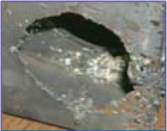
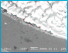
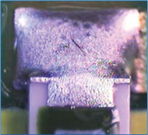
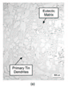
What was not realised was that there is a temperature that a metal surface has to reach before the wetting reaction required to form a joint can proceed that is not directly related to the melting point of the solder. The process temperatures used with tinlead solder were therefore determined more by that temperature than by any concept of ‘superheat’. Thus wave soldering with lead-free alloys can proceed at much the same temperatures as have been used with tin-lead solder, typically around 255-260°C for both tin-silver-copper and modified tin-copper alloys and reflow peak temperature are typically 10°C lower than predicted. New equipment is needed for lead-free soldering. The higher melting point of the lead-free solders is not entirely free of implications for soldering processes. The difference between the process temperature and the melting point is much smaller for leadfree solders than it has been for tin-lead solder and that means that there is a much smaller ‘process window’ in which to operate. However, for reasons that have nothing to do with any future change to lead-free, most modern soldering equipment that had been designed for tinlead solder already had the capability of maintaining process parameters within the narrower range required for lead-free processes. Some older equipment with limited process control capability may not be suitable but in many cases it has proved possible to run lead-free processes with simple upgrades, e.g. adding extra preheat modules to a wave soldering machine. A controversial aspect of equipment compatibility with lead-free soldering is solder pot erosion. Molten tin will react with and dissolve most metals including the metals used for the construction of soldering equipment. The aggressiveness of tin in that regard was considerably diminished by its one third dilution with lead in conventional tinlead solder but erosion of stainless steel could still occur if the protective oxide film is penetrated mechanically or chemically. Whether or not molten lead-free solder will erode stainless steel machine parts depends on its composition and practical experience indicates that there is a considerable difference between alloys in that regard. The presence of silver in the solder appears to disrupt the protective oxide film making these alloys more likely to cause erosion of machine parts. If, as is usually the case, the tin-silver-copper alloy also has phosphorus added as an antioxidant then the protective oxide film is quickly penetrated and damaging erosion follows. If these alloys are used, then it is necessary to use equipment in which stainless steel parts exposed to molten solder are treated or coated to make them more resistant to such attack or which is lined with or constructed from metals such as titanium that are more resistant to such attack. It is not important that a solder behave as a eutectic. Given that it is within the memory of many people still working in the industry that electronics manufacturers accepted an approximately 5% increase in cost to move from ‘60/40’ (60% tin, 40% lead) to ‘63/37’ to get an alloy that behaves like a eutectic alloy it is surprising that in the move to lead-free there was not more emphasis on finding alloys that behave as a true eutectic. Purists will point out that the true tin-lead eutectic is actually at 61.9% tin but given the tendency to lose tin by oxidation and reaction with substrates a little more quickly than lead it was found worthwhile erring a little on the high tin side. Certainly the industry consortia in Europe and North America homed in on two alloys of nominal eutectic composition, Sn with about 0.7% Cu and Sn with around 3.8-3.9% Ag and 0.7-1% Cu (there being some difference of opinion about the composition of the Sn-Ag-Cu eutectic). However, in their unmodified form neither of these alloys behaves as eutectics. To understand the consequences of non-eutectic behaviour it is necessary to consider the difference in the way eutectic and noneutectic alloys solidify. The distinguishing feature of a eutectic is that the two or three (or more) constituent phases freeze from the melt simultaneously and isothermally in a process known as ‘coupled growth’. Since the freezing is isothermal a eutectic behaves like a pure metal except that the solid that is forming is made up of several different phases rather than the elemental metal. From each nucleus of solid that forms within the liquid at the melting point individual solid phases grow almost in parallel with the microstructure controlled by the rate at which the elements in the liquid can separate themselves out. The classic binary eutectic is tinlead since the lead-rich and tin-rich phases grow as closely spaced parallel plates. The gross manifestation of this eutectic microstructure is a joint with the smooth bright crack-free finish of a well made tin-lead solder joint. When an alloy in a eutectic system is of non-eutectic composition the solidification of the eutectic is preceded by the precipitation of a primary phase which has a lower content of alloying elements than the melt from which it is solidifying. The consequence is enrichment of the remaining liquid in those elements until it reaches the eutectic composition when it freezes. The outward manifestation of the resulting microstructure is the rough grainy surface left as the eutectic shrinks away from the network of primary dendrites or intermetallic crystals. Depending on the way the solidification front moves through the solder deep shrinkage cavities can be left that have been found to be points of crack initiation in vibration testing.
Neither of the two alloys recommended by industry consortia in Europe and America, tin-copper and tinsilver- copper freeze as true eutectics in their unmodified form and the result is the predicted grainy and often cracked finish. There can be nothing more to lead-free solder formulation than mixing the basic constituent elements.
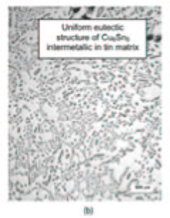
Perhaps because tin-lead alloy worked so well as a solder without any further modification the electronics industry did not initially give consideration to the possibility that the ‘less than ideal’ behaviour of the candidate lead-free solders could be improved. In the foundry industry, however, the concept of improving the performance of an alloy by trace level additions was well established and widely employed. Aluminium internal combustion engines, for example, are possible only because of successful modification of the aluminium-silicon eutectic alloy on which they are based. To understand how candidate lead-free alloys could be modified to improve their performance as solders it is necessary to look more closely at how they differ from tin-lead solder. A significant difference between these lead-free solders and tin-lead in that the other phases in their eutectics are intermetallic compounds rather than simple metallic solid solutions. Although the tin-rich and lead-rich phases in the tin-lead eutectic are crystalline they do not grow in a form that is recognisable as crystalline. By contrast the intermetallic compounds in the Sn-Cu and Sn-Ag-Cu systems, Cu6Sn5 and Ag3Sn grow in a faceted manner to form structures that are distinctly crystalline in appearance, needles in the former case and plates in the latter. Probably because that faceted growth is difficult to nucleate, the coupled growth that is characteristic of a eutectic America, tin-copper and tin-silver-copper freeze as true eutectics in their unmodified form and the result is the predicted grainy and often cracked finish.
Download this article - Fact and fiction in lead-free soldering - Part I
|